Neuro N6 Getting Started
The Neuro N6 development board, its main components and connectors, and the steps to first operation.
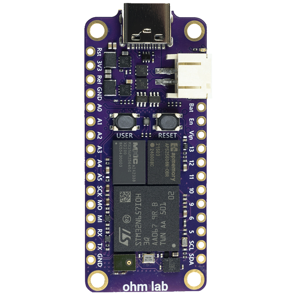
The Neuro N6 is a development board by Ohm Lab built around the STMicroelectronics STM32N657I0 microcontroller. The STM32N657 combines an Arm Cortex-M55 core at 800 MHz with an ST Neural-ART accelerator at 1 GHz, rated at 600 GOPS. The board adds external PSRAM and flash, a USB-C interface, two board-to-board connectors for expansion modules, an inertial unit, a magnetometer, a microphone, an RGB LED and a user button, in an Adafruit Feather compatible form factor. Camera modules attach through the board-to-board connectors and add the camera, and depending on the module a strobe LED, a time of flight sensor, a display with touch and speaker, or a wireless module.
Specifications
| Microcontroller | STM32N657I0 in VFBGA178 (12 x 12 mm, 0.8 mm pitch, 106 I/Os). Cortex-M55 at up to 800 MHz in overdrive, 32 KB instruction and 32 KB data cache, Helium vector extension, half, single and double precision FPU, TrustZone |
| Neural accelerator | ST Neural-ART, up to 1 GHz, 600 GOPS, 288 MAC per cycle, stream processing engine, on-the-fly weight decompression and encryption |
| On-chip RAM | 4.2 MB contiguous SRAM with ECC, 128 KB data and 64 KB instruction tightly coupled memory with ECC, 8 KB backup SRAM retained in VBAT mode |
| External RAM | 64 MB OctoSPI PSRAM (AP Memory APS51208N), 200 MHz clock |
| External flash | 32 MB OctoSPI flash (Macronix MX25UM25645G), 200 MHz clock |
| Camera pipeline | DCMIPP with image signal processor and three parallel pipes, rated for sensors up to 5 MP at 30 fps. CSI-2 version 1.3 host, two data lanes at up to 2.5 Gbit/s per lane |
| Video and graphics | VENC hardware encoder: H.264 up to 1080p at 15 fps, JPEG up to 300 Mpixel/s. Neo-Chrom 2.5D GPU, Chrom-ART DMA2D, LCD-TFT controller with two layers up to XGA |
| USB | USB-C, USB 2.0 OTG high speed 480 Mbit/s with internal PHY |
| Board-to-board connectors | One 30-pin and one 40-pin, 0.4 mm pitch: MIPI CSI-2, RGB565 LCD, SDMMC, four-wire UART, I2C, SPI, SAI, SWD, power |
| On-board sensors | LSM6DSL six-axis inertial unit with temperature sensor, MMC5603NJ three-axis magnetometer, MP34DT05-A PDM microphone |
| Indicators | User programmable RGB LED, charging status LED |
| Input | USER button, reset button |
| Header | Adafruit Feather pinout: SPI, I2C, UART, six analogue inputs with ADC, seven digital inputs and outputs, and the Feather power pins USB, BAT, 3.3V, AREF, EN and RST |
| Power | USB-C, 5 V on the header USB pin, or a single cell 3.7 V lithium ion or lithium polymer battery through a JST-PH connector. 500 mA charger |
| Debug | Six-pin connector with SWDIO, SWCLK, NRST and boot pins. The MCU provides serial wire and JTAG debug and an Embedded Trace Macrocell |
| Operating range | MCU supply and I/O 1.71 to 3.6 V (3.3 V on this board), junction temperature -40 to 125 C |
| Dimensions | 53.04 x 22.83 x 8.85 mm, 6.7 g |
| Part number | OL-DEV-N6-001, hardware revision C |
| Design licence | CERN-OHL-S v2. The schematic is published in the Neuro-N6-Hardware repository |
The STM32N657 is documented in ST datasheet DS14791, reference manual RM0486 and errata sheet ES0620.
Contents of the package
A Neuro N6 board. Camera modules and cables are supplied separately or as a kit. See the product pages for Neuro Vision OV5640 and OV5640-W, Neuro Vision STCam, Neuro Vision Thermal and Neuro Vision TFT and TFT-W. The -W variants carry the WiFi and Bluetooth LE module.
First operation
- A camera module is mated to the two board-to-board connectors, with the board unpowered.
- The board is connected to a computer with a USB-C cable that carries data.
- The RGB LED lights purple, indicating that the application has started, and the board enumerates as a USB serial device named Neuro N6.
- The Arduino core is installed and the Blink example uploaded. See Software Getting Started.
Indicators
| LED | State | Meaning |
|---|---|---|
| RGB | Purple | Application running, LED not yet written by the sketch |
| RGB | Slow red pulse | Bootloader mode |
| RGB | Solid red shortly after power up | Firmware error handler. The serial port prints a diagnostic |
| RGB | Off | The sketch has turned the LED off, or the power save library is active |
| Charging status | Red, on | Battery charging |
| Charging status | Red, flashing at 20 Hz | USB connected, no battery connected |
| Charging status | Off | Battery fully charged, or no USB connected |
The charging status LED is not programmable.
Buttons
The USER button is readable from a sketch and reads HIGH while pressed. The reset button resets the microcontroller and peripherals; two presses less than 900 ms apart enter the USB bootloader, which does not depend on the application and recovers a board with a corrupted sketch. See LEDs and the Button.
Boot modes
| Mode | Entry | Use |
|---|---|---|
| Boot from flash | Default | The STM32N6 boot ROM loads the FSBL from the XSPI flash, and the FSBL loads the application into RAM |
| Ohm Lab bootloader | Upload from the Arduino IDE, or a double press of reset | Programming the application and model weights over USB-C |
| ST serial boot | BOOT0 asserted on the debug connector during reset | The boot ROM accepts an image over USB or UART. Not supported by Ohm Lab tooling |
| ST development boot | BOOT1 asserted on the debug connector during reset | The boot ROM reopens debug and idles. Used for STM32CubeIDE debugging, programming flash with STM32CubeProgrammer and the external memory loader, and recovery of a corrupted FSBL |
The STM32N6 has no internal flash and always boots from its ROM, which authenticates the first stage image. BOOT0 is a dedicated pin latched at reset release; BOOT1 is a configurable pin. The FSBL occupies flash from 0x90000000 to 0x90100000 and must not be overwritten. See Uploader and Bootloader.
Handling
Header logic is 3.3 V with an absolute range of -0.3 to 3.6 V and a board-rated current limit of 4 mA per pin. The analogue inputs are limited to 1.8 V, the ADC's reference supply. Only one 5 V supply is connected at a time; connecting USB-C and a second supply on the USB pin causes supply contention. Only a rechargeable 3.7 V single cell battery is connected to the battery connector. The board-to-board connectors carry high speed differential signals and are mated only with the board unpowered. The board and the charger may become warm during heavy operation and charging.
Related pages
Board Tour and Pinout describes each connector and pin. Power and Battery describes the power path, electrical limits and battery operation. Downloads lists design files. Regulatory Compliance records the board's compliance status.